
The new Sony Alpha A9 III camera is the first commercial stills-orientated camera with a global shutter function incorporated into the sensor, allowing the exposure integration time (when light is being collected) to start and finish simultaneously for all pixels in the sensor.
Some of the benefits of the global shutter are that the A9 III allows shutter speeds up to 1/80,000 second, with flash synchronisation at all speeds. But amidst all the hype, one question has gone unanswered: how does the Sony A9 III global shutter work?
The short answer is that the global shutter sensor requires two photodiodes for every pixel. Alongside the one that captures the light, there’s another to temporarily store the accumulated charge before it’s read out. However, this second one restricts the capacity of the first, which neatly explains why the A9 III’s ‘base’ sensitivity is limited to ISO 250, compared to ISO 100 on the A9 II. Read on for the full technical details.
How does a conventional electronic shutter work?
To understand how a global shutter works, we first have to understand the function of a ‘normal’ pixel, using the four-transistor architecture shown in figure 1 below. Here three of the transistors act as switches (TG, RST and RS) and are shown as such in the diagram. The other acts as an amplifier (SF), shown using the triangular amplifier symbol. The other functional components in the pixel are the photodiode (PD) and a capacitor (FD).
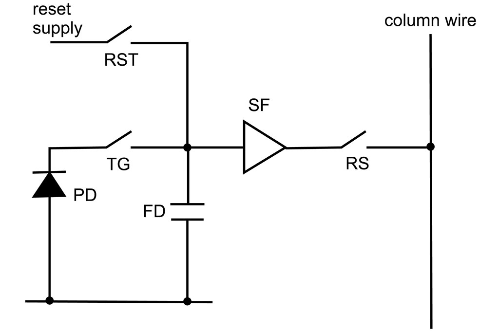
Figure 1: circuit diagram of a conventional CMOS sensor pixel. Credit: Prof Bob Newman
A capture starts with the closing of the RST and TG switches, which connects the photodiode and FD capacitor to the reset supply, clearing any charge that they hold. The exposure starts when both switches are opened, isolating the photodiode and allowing it to accumulate photocharge. It does this until it is read out. The reading process entails closing the RS switch, which connects the output of the SF amplifier to the column line, from where it is directed to the digitisation circuitry. This happens twice for each read operation.
Firstly, the reset level in the FD capacitor is read out. After that the TG switch is closed, allowing the accumulated charge in the photodiode to flow into the capacitor, where it changes the voltage across the capacitor, according to the amount of charge and size of the capacitor. This voltage is sent to the column wire by the SF amplifier, and the pixel value is the difference between that reading and the one of the reset level. This process, called ‘correlated double sampling’ greatly reduces the pattern noise produced by the sensor, by ensuring that only accumulated charge is counted.
Since the column wire is shared by every row of pixels, only one row can be read out at a time. It is the read-out that determines the end of the exposure. Thus to provide a uniform exposure time the exposure must be started line–by-line, a constant time before each row’s read-out – thus resulting in the ‘rolling shutter’ or ‘Jello’ effect.

The Sony A9 III’s new image sensor provides the first global shutter in a consumer camera. Credit: Sony
How does the Sony A9 III global shutter work?
To provide a global shutter, all rows must start and stop exposure at the same time, which means that there must be somewhere to store the pixel charge until the row can be read out. How this is done is shown in figure 2. Another photodiode (not exposed to light) is added to the circuit, labeled SD in the diagram, along with another switch (SG). Now when the exposure is finished SG can be closed to transfer the photocharge to SD, where it is stored until the pixel can be read out.
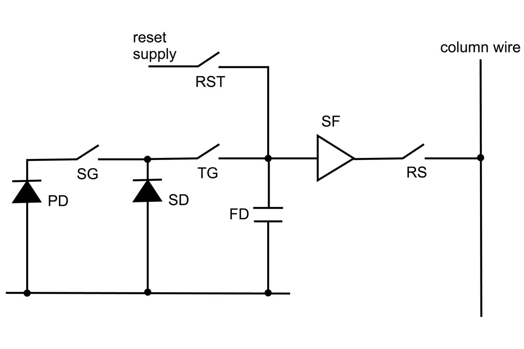
Figure 2: Circuit diagram of a global-shutter CMOS sensor pixel. Credit: Prof Bob Newman
The disadvantage is that the additional photodiode, which plays no part in light collection, restricts the charge capacity of the main photodiode. This has the effect of reducing the maximum exposure that the sensor can collect, and thus increases the ‘base ISO’. The A9 III has a lowest ISO of 250, and thus can handle less light than can the older A9 II, or indeed an APS-C camera with a base ISO of 100. Moreover, the extra circuitry in the pixel precludes the inclusion of the circuitry needed for the dual conversion gain feature, which has become the norm for top-end cameras. This provides two alternative pixel readout-circuits to minimise electronic read noise at both low and high ISO settings.
In the context of a specialist sports-action camera such as the A9 III this is not a major issue, as the camera is likely to be mainly used at high ISOs. For a more general-use stills camera it might be.

Professor Bob Newman
Bob Newman is currently Professor of Computer Science at the University of Wolverhampton. He has been working with the design and development of high-technology equipment for 35 years and two of his products have won innovation awards. Bob is also a camera nut and a keen amateur photographer.
Related reading:
- Are smaller pixels worse? Sensor technology myths explained
- In praise of Bryce Bayer and the supreme Bayer Sensor
- Sensor size MFT vs APS-C vs Full-Frame
Follow AP on Facebook, Twitter, Instagram, and YouTube.